


The name behind the patent for the printed circuit board is Paul Eisler from 1943. However, the invention happened in the early 1900s, somewhere in 1903. Since then, it has gone beyond those initial phenolic substrates. Initially, the PCB assembly was solely done by hand and slowly shifted to using microscopic components placed with surface mount technology or SMT assembly. Talking about the present time, it is more about something high-density interconnect platforms, which are multilayered and are present in any next-designed electronic product.
With the impact of growing technology, a printed circuit board is expected to do more than just carry superior signal speeds, better power density, and more, while also working to lower costs and meet sustainability targets.
You must be wondering how something like PCB can be evolved and how it can help procurement and engineering teams.
Types Of PCB
Rigid Boards
If you are dealing with high-reliability electronics, this workhorse technology is for you. You will find it covered in several layers of laminated material. To start with, you will get high Tg variants or glass-reinforced epoxy substrate, copper foil, solder mask, followed by silkscreen. With extreme heat and pressure, these layers are bound together.
Generally, if you end up discussing the varieties of printed circuit boards with any OEM or original equipment manufacturers, they will ask you to focus on usage and requirements. Often, they say, a rigid construction keeps dominating with dimensional stability, steady performance, and mechanical robustness, but needs time-to-time replacement or care. Regardless of the area in which it is utilised – industrial, medical, or safety – it must be properly maintained to avoid any unwanted situations.
These PCBs might face exposure to humidity and fluid, mechanical shock, changes in temperature, vibrations, and more from time to time. If the rigid PCB assembly is done with care and the right materials are used, it can withstand stress at any level. Even when heat and mechanical loads are applied, it can function well. It is highly recommended for X-ray machines, CT scanners, MRI systems, and other medical imaging devices. At these places, you need a more reliable system, and a rigid PCB is indeed one. Even in an industrial sector, it works well in power conversion, telecom infrastructure, automotive ECU, and more. It is an ideal choice for these industries where you need something to run for a long time without incurring additional costs for replacement.
Flexible and Rigid Flex PCB
Rigid PCBs are indeed powerful, but that does not mean flexible PCB demand is not growing. These are developed on polyimide or sometimes flexible substrates and are made in a way that they can be folded, twisted, or even bent with ease, all within the enclosure. Their biggest quality is their ultra-thinness and lightweight design, which allows them to be placed at interconnects via hinged or moving assemblies. You can see them being used in aerospace for avionics, satellite payloads, navigation, medical devices, such as smartwatches, minimally invasive tools, automotive interiors for lighting, steering wheel and motion control, and industrial robot systems.
Flex circuits come with additional advantages in aerospace as they offer high resistance to radiation, high temperatures, vibration, and shock for controlling weight, which is mandatory for anything that is set to fly. It has everything an aerospace company needs, including temperature sensors, control tower instrumentation, and more. Flexible ones are more focused on interconnecting with mission-critical functionality.
Miniaturisation, Advanced, and HDI Assembly
Nowadays, people are more inclined to invest more in something smaller, more capable, and lighter devices. Today, there are several sophisticated electronics on the market. PCB designers have introduced high-density interconnect features, including microvias, space-optimised geometries, via-in-pad for high-pin-count applications, and blind and buried vias. This ensures that more features can be introduced into smaller boards with reduced power consumption and better signal integrity. This makes the PCB assembly process a bit challenging, as the pad size needs to be shrunk, placed closely together, and the tolerance must be tightened. All these features help in:
- AOI or Automated optical inspection and X-ray strategies
- Component handling
- Placement accuracy
- Fixed paste deposition back with stencil design
- Thermal management
- Reflow profiles
If this PCB work with the right efficiency, it can prove more reliable. They are thin and can support an interconnected length, resulting in the board being more tolerant to shock, thermal cycling, and vibration. The biggest perk is that these boards do not require drilling holes for placement and can be placed directly. This helps overcome several mechanical challenges associated with old through-hole technology. This circuit board has to be designed when one starts designing a product. If DFT or DFM is handled carefully at this point, extra charges can be controlled.
Sustainability and End-Of-Life
The oldest FR-4 printed circuit boards are not that simple to recycle. The primary reason is the material used in its development. Epoxy resin, material layers, and glass fibre are tough to recycle. The valuable and reusable components used in it, such as gold, copper, tin, and other metals, require extraction to be important here. It not only helps them in meeting the supply chain but also fetches economic returns.
Nowadays, with the ongoing pressure from environmentalists and industry leaders, manufacturers are focusing on creating something which is more environmentally friendly. People are also exploring paper-based PCBs, where conductive inks can be printed onto a paper substrate. Natural fibres or encapsulated materials are used here to make the board, as they are non-toxic polymers that can be easily mixed in hot water. In this case, the recoverable component and the compostable organic material can be extracted easily. Here, the focus is not budget-specific, but rather on the three R’s: reuse, recycle, and reduce.
In the modern technological world, the new PCBs that are emerging come with these innovations, which are expected to become better with time:
- Upfront process for disassembly
- Using quality parts which are easy to repair and simple to upgrade
- Buy from the manufacturer who has a set method for recycling and material recovery.
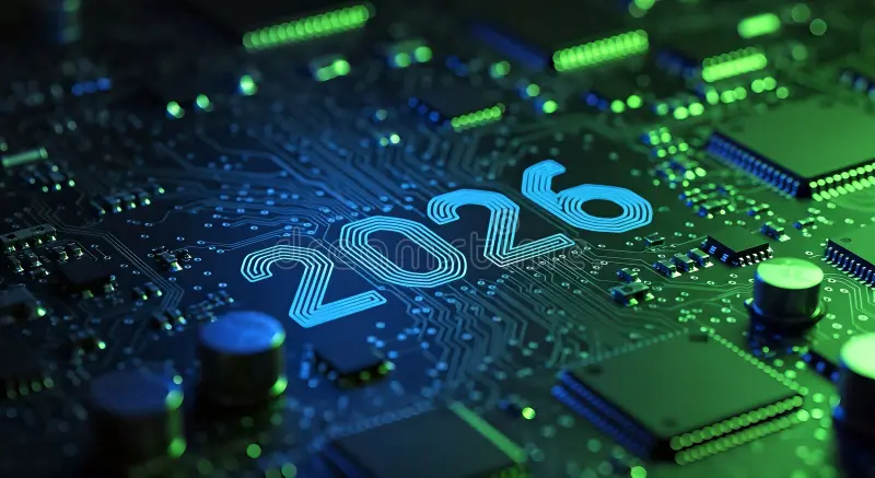
Expected Growth Rate of PCB Manufacturing in 2026
It should now be clear to you that the role of PCB has expanded to encompass every sector of electronic manufacturing. This clearly indicates that the growth of this market is likely to grow more with every passing day. As per the New Wires report, the printed circuit board market might surpass $72.3 billion by the end of 2026. Electronic vehicles have contributed significantly to this growth, alongside other automotive features such as ECU systems, GPS capabilities, and anti-lock brake systems.
Wrapping Up
PCB has already expanded its market and backed this up with the fact that no more cost-effective alternative is available to it; therefore, the growth of this market is likely to arise. With its extensive customisation scope, ready availability, rising EV adoption, 5G market, flex circuits, and more, the market’s potential is incomparable.